An ISA to Parallel Port Interface & Circuit.
There is a lot of confusing information to be gleaned from the internet regarding the conversion of old ISA cards for use in a modern computer. About 25 years ago I had designed a plug in ISA card which provided me with a dual channel sampling oscilloscope, the intention being to have this as a backup to manufacture in the event I ran short of work. In the mean time as the years rolled by I used the ‘scope to good advantage. Along the way I managed to also accumulate several updated desk top computers as new improved versions became available. In the end I decided it was time for a clear out but my very old desk top was running the ISA main board and my trusty oscilloscope. Thus there came a need to make the ‘scope operate from the Parallel Port so I could junk the old PC.
I shall not repeat all the stuff regarding Parallel ports gleaned from the internet, but just to add to the confusion by elaborating on how I managed to interface the old ISA card using the circuit attached. There appears no easy solution to convert an ISA card for use on a none ISA computer and from the web comments there are plenty of ISA cards still in use.
First let me say that modern desk top computers are much too fast to be able to adapt the PCI bus for a simple conversion. I had tried my old Pascal v7 software but this balked with the 'run time error 200' so I used the 'patchcrt' available patch which solved the problem, many thanks to the author. Even the parallel port is much faster than the old ISA bus running anywhere up to 2 Mhz. When I finally got this interface completed, I measured the port Dstrobe pulse at 0.5 uSecs.
All the information regarding the port may or may not be correct depending on your PC version and its age. This was the biggest problem initially to sort out. Do not accept all you read about the ports operation as PC motherboards are not standard in manufacture & you will definitely need to write some test programs to evaluate what you have available. In addition you will need the source program of your own card in order to insert the changes needed from the single 16 bit ISA Read/Write operation to the four revised separate operations needed for the interface card. Also, you may need to use part of the available 16 bit addresses lines to provide the old ISA signals: AEN, IOR & IOW which can be emulated by programing.
Here are some of my test results in EPP mode.
Notes Re the Parallel port signals.
FACT: Xp/Win7 Dos did not allow control regs to be changed, needs Dos 6.
FACT: WRITE & DSTROBE are high before any transfers were tried.
FACT: On Pc switch on, bit 5 is at 1 for inputs and DSTROBE is Hi and ready.
FACT: Tests to write control register bit 5 low for outputs succeeded( XOR 32 with Control register read value).
FACT: ASTROBE is not already hi, why ? (Fortunately not really needed as Dstrobe will send addresses and data).
FACT: Data outs using Address register & Dstrobe worked ok.
FACT: Read inputs using Address register needs < 680 ohms to force test logic zero. No Astrobe present.
FACT: Register at 37Ch (892) writes Data properly, 37Ah(891) failed, does this need setting separately?
FACT: Address & Data registers did not auto write two successive outputs, just the data register outputs.
The Address Port can be Read or Written to at Base Address + 3 = 37Bh or 891 dec , Dstrobe signal active.
The Data Port can be Read or Written to at Base +4 = 37CH or 892 dec, Dstrobe active. Testing wrote & read back the same values to the Address register. .
The only way to get the Rs signal to work was to change the line to an output (=Low) and then back to an input(=High). I was unable to change to an output then go from low to high by writing to the control port.
If INT is set low by the peripheral then the Host is interrupted(not tried).
In the end I settled for writing/ reading as four single operations using the data register as a means of transferring bytes. This gave 16 bit addressing and 8 bit data. Test programs need to be used before hardware construction begins to confirm that your coding will operate as desired, these were compiled using Pascal v 7. Here are the programs used for the interface. When ever a read or write was required a call to Conout or Conin (below) was made to make sure bit 5 was set properly. If you change the variables name, ensure that you have not inadvertantly used an existing name in the source program. IE I used Flag5 because the source program already had Flag1 to Flag4 as variables.
Using Pascal v 7 (patched).
Variables Datin,Datout,Ctrl:byte;
Flag5:Integer;
Procedure Bit5; {Test for epp in/out direction}
Begin
If Ctrl >127 Then Ctrl:= Ctrl - 128; {Bit 7 present}
If Ctrl > 63 then Ctrl:= Ctrl - 64; {Bit 6 Present}
If Ctrl > 31 Then Flag5:= 1 {Bit 5 is set for inputs}
Else Flag5:=0;
End;
Procedure Conout; {Set P Port bit 5 for outputs}
Label Cout;
Begin
Address := 890; {Control Port}
Datin:=Port[Address]; {Get data}
Bit5; {Check bit 5}
If Flag5 = 0 Then goto Cout; {Bit 5 is already set for output}
Ctrl:=Ctrl XOR 32; {Invert bit 5}
Port[Address]:=Ctrl; {Set control for output}
Cout: End;
Procedure Conin; {Set bit 5 for inputs}
Label Cin;
Begin
Address := 890; {Control Port}
Ctrl:=Port[Address]; {Get data}
Bit5; {Check bit 5}
If Flag5 = 1 then goto Cin; {Bit 5 is already set for output}
Ctrl:=Ctrl XOR 32; {Invert bit 5}
Port[Address]:=Ctrl; {Set control for output}
Cin: End;
Procedure Out892;
Begin
Address:=892;
Port[Address]:= Datout;
End;
Procedure Inp892;
Begin
Datin:=0;
Address:=892;
Datin:= Port[Address];
End;
Each in or out operation takes about 5 uSecs or 20 uSecs overall. IE Write address 1, write address 2, write Data 3 & final write 4. (See interface circuit & notes). In the source program, each old ISA Read/Write single operation was replaced by the four separate operations. That meant searching for inputs and output commands and evaluating the 16 bit address value so that the code could be broken down into the two 8 bit addresses from the original. For example a 12 bit address 263 would need to be separated into codes of 255 and 8 for each of the two address writes. If the original source code also made use of the IOR, IOW & AEN control lines then these also need to be provided using any spare address lines.
In summary the control signal used for the interface were Ds, Wait, & Rs. Address bytes & Data byte all sent from the Data register(892).
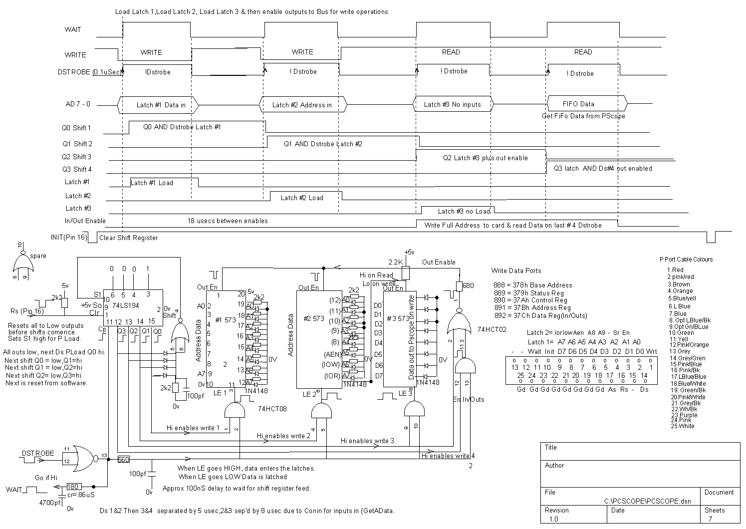
Interface Operation.
1) The Rs signal is outputted to initialise the shift register. Each of the shift register outputs are set to zero which sets S1 high ready for the first write. Address A0 - A7 Data is loaded into base register +4 (892) & then outputted. The leading edge of Ds will parallel load & set Q0 high, this also sets S1 low ready for the next Ds and enables storage register #1. The WAIT signal goes high after a small delay. Data is latched into the storage register when Ds returns high after about 0.5 uSecs. That completes Write #1.
2) The second Ds signal shifts Q0 low & Q1 high enableing storeage register #2. Address Data is latched into register #2 completing Write #2.
3) The third Ds signal shifts Q1 low & Q2 high enableing storeage register #3. Data is latched into register #3 completeing Write #3. Well not quite...In actual fact register #3 could be dispensed with if you are satisfied that both addresses and data will do their job within the 0.5 uSecs. This might be a problem for slow responding circuitry in which case this configuration will output the addresses & data until the final Ds is completed.
4) The fourth Ds signal shifts Q2 low & Q3 high maintaining the outputs until the Ds signal ends. This provides an output for a full 5 uSecs for the card to complete its operation. #4 write completes the sequence.
Delaying the WAIT signal did not widen the Ds signal. If the WAIT signal is kept low then the Ds signal ends.
The parallel Port cable used was the standard Centronics printer cable. This had a tendency to ring as signals were transferred so diodes & resistors were included to stabilise the address & data transfers. To protect the port from inadvertant damage due to simultaneous data outputs from both the card & port, 270 ohm resistors were placed in the port data lines.